Gan Mosfet

Gan Stmicroelectronics

Sciencecentral

Normally Off Al2o3 Gan Mosfet Role Of Border Traps On The Device Transport Characteristics Sciencedirect
Tesla On Board Gan Gallium Nitride Charger Teslamotors

Panasonic Showcases Gan And Sic Mosfet Advances

Si Vs Gan Vs Sic Which Process And Supplier Are Best For My Power Design Edn
GaN FETs Efficient and effective highpower FETs Getting the right power density while ensuring the best repetitive Safe Operating Area (SOA) and delivering both device and thermal efficiency, requires a specific mix of capabilities and expertise When it comes to very high efficiency and highpower density, then Nexperia’s 650 V GaNonSi FETs offer an ideal solution.
Gan mosfet. GANWSA The GANWSA is a 650 V, 50 mΩ Gallium Nitride (GaN) FET It is a normallyoff device that combines Nexperia’s stateoftheart highvoltage GaN HEMT and lowvoltage silicon MOSFET technologies — offering superior reliability and performance. Gallium Nitride (GaN) is a hard and stable substance that is revolutionizing semiconductors for military communications, radar, and electronic warfare SSDI specializes in offering fully screened GaN products in hermetically sealed packaging Contact the factory to inquire about modifications or other requirements 11 Item (s). GaN devices allow gate charge reduction without sacrificing onresistance, leading to power savings and total system downsizing ST and GaN ST started working on wide bandgap materials (WBG) in 1996 with SiC MOSFETs and SiC diodes and has become one of the main players in the market We are now expanding our portfolio of wide bandgap power products with the 650V & 100V normallyoff GaN Highelectronmobility transistor (HEMT) devices.
GaN brings all the benefits of solidstage devices, such as precise control, reliability and ease of use to RF energy while also offering improved RF performance when compared to legacy vacuum tubes and magnetrons RF Power Solutions Overview 5G Integrated Solutions. VisIC’s industryleading GaN power transistors are the building blocks of unparalleled efficiency gains in the powertrain of electric cars The D 3 GaN technology semiconductors allow for smaller, lower cost, more efficient systems, extending the range of electric cars. Overview Microsemi RF Power Transistor product portfolio includes Silicon Bipolar Junction Transistors (Si BJTs), Silicon MOSFETs, and Gallium Nitride GaN Transistors for Avionics, Radar, Semiconductor Capital Equipment, Welding, Medical, Communications, Defense and Space Applications.
GaN FET Drivers 3 Products Parametric Search Parametric Search Description Configuration Max Vin (V) Frequency (MHz) Rise Time (ns) Fall Time (ns) Propagation Delay (ns) Min Output Pulse Width (ns) Deadtime Control Features Package Package (mm) PE PE Highspeed FET Driver High and lowside FET drivers. GaN Breaks Barriers – RF Power Amplifiers Go Wide and High As shorter gate length GaAs and GaN transistors become available, coupled with improved circuit design techniques, new devices are becoming available that can perform comfortably to millimeter wave frequencies, opening new applications that were hard to contemplate a decade ago. GaN Systems GaNonSi MOSFET are available at Mouser Electronics Mouser offers inventory, pricing, & datasheets for GaN Systems GaNonSi MOSFET.
Our SiC MOSFETs replace silicon devices to enable lower switching and conduction losses with higher blocking voltages and avalanche capability We established a new benchmark for energyefficient power switches when we created the industry's first fullyqualified silicon carbide MOSFET in 11, and we have been perfecting the technology ever since. GaN FET gate drivers Highspeed GaN gate drivers enabling high power density and design simplicity for every power topology Our drivers’ combination of fast timing specs, leadless packages, and narrow pulsewidth response enable you to switch FETs fast. Yet it maintains the improved voltage blocking characteristics and switching performance of a naturally “on” GaN HEMT Having a tunable lowvoltage MOSFET in series of course does technically increase the R DS(on) and Q RR of a cascodemode device However, these increases are minimal or even inconsequential, especially when contrasted.
GaN brings all the benefits of solidstage devices, such as precise control, reliability and ease of use to RF energy while also offering improved RF performance when compared to legacy vacuum tubes and magnetrons RF Power Solutions Overview 5G Integrated Solutions. Before gallium nitride (GaN), the silicon (Si) MOSFET was the standard for power in adapter applications for decades As a result, many of the existing controllers in the marketplace, including power factor correction (PFC) and DCDC controllers, have already integrated silicon drivers into the controller chip. News Alpha and Omega Semiconductor Releases Fast Switching 600V αMOS5™ Super Junction MOSFETs in SMDtype TOLL Packagemore »;.
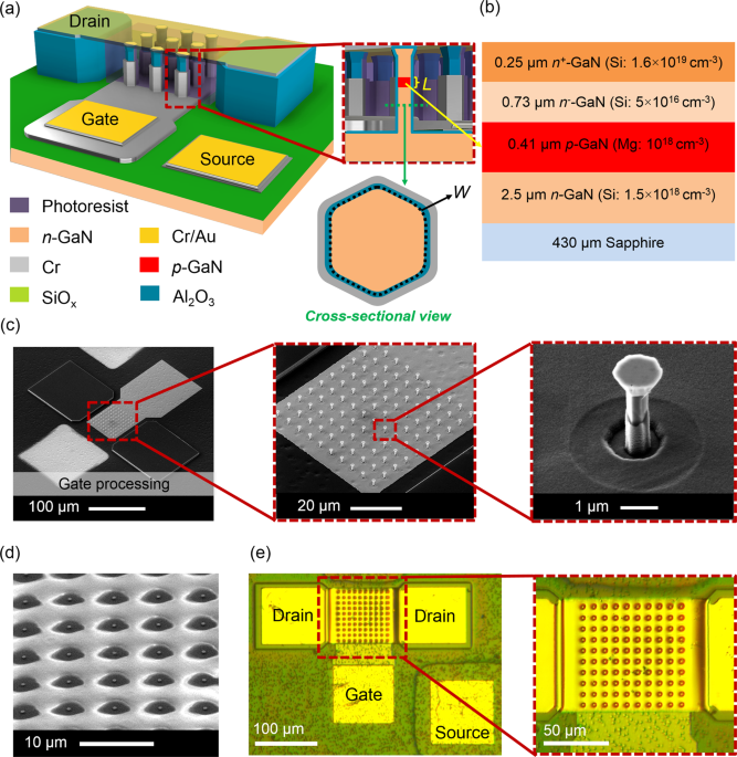
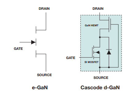
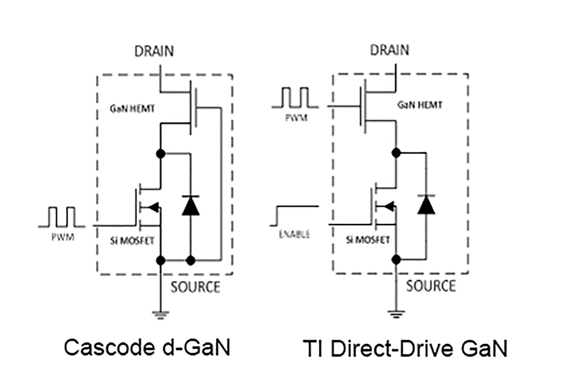
GaN transistors used for power conversion can be classified into cascode and pGaN gate types The cascode type is combined with a GaN HEMT and low voltage silicon MOSFET in a single package The pGaN gate type uses a pGaN gate to make GaN HEMTs normallyoff. On a simple transistortotransistor basis, GaN was significantly more expensive resulting from low volume production and low yields As an immature product, the industry was also not sure how to prove the reliability of GaN devices It was unclear if the JEDEC MOSFET test standard was appropriate or sufficient. The cascode type is combined with a GaN HEMT and low voltage silicon MOSFET in a single package The pGaN gate type uses a pGaN gate to make GaN HEMTs normallyoff Toshiba’s new GaN cascode is less susceptible to noise, a source of malfunction, as it has a higher threshold voltage than pGaN gate normallyoff HEMT devices.
What is the benefit in driving negative if it's not required?. GaN FET gate drivers Highspeed GaN gate drivers enabling high power density and design simplicity for every power topology Our drivers’ combination of fast timing specs, leadless packages, and narrow pulsewidth response enable you to switch FETs fast. A gallium nitride (GaN)based normally off metal–oxide–semiconductor fieldeffect transistor (MOSFET) using a dualmetalgate (DMG) structure was proposed and fabricated to improve current drivability Normally off operation with a high Vth of 23 V was obtained using a Cl2/BCl3based recess etching process The DMG structure was employed to improve current characteristics, which can be.
Gallium nitride (GaN) continues to ramp into $B silicon chip market DUBLIN, Ireland (PRWeb) Navitas Semiconductor today announced they have been awarded ASPENCORE’s Electronic Products’ “Power Product of the Year” Navitas’ GaN Power IC NV612x series was. Overview Microsemi RF Power Transistor product portfolio includes Silicon Bipolar Junction Transistors (Si BJTs), Silicon MOSFETs, and Gallium Nitride GaN Transistors for Avionics, Radar, Semiconductor Capital Equipment, Welding, Medical, Communications, Defense and Space Applications. Qorvo offers a broad portfolio of gallium nitride (GaN) discrete transistor products with varying levels of power, voltage and frequency ratings, in both dielevel and packaged solutions Our products provide the high performance of GaN plus the convenience of industrystandard packaging, which speeds design and manufacturing — all backed by.
GaN FET GaN switching devices are available in two different types enhancement mode (eGaN) and cascoded depletion mode (dGaN) An eGaN works as a normal MOSFET, even if it has a reduced gatetosource voltage It offers a simpler package, a low resistance without a body diode with the bidirectional channel that behaves like this. GaN FET GaN switching devices are available in two different types enhancement mode (eGaN) and cascoded depletion mode (dGaN) An eGaN works as a normal MOSFET, even if it has a reduced gatetosource voltage It offers a simpler package, a low resistance without a body diode with the bidirectional channel that behaves like this. GaN Breaks Barriers – RF Power Amplifiers Go Wide and High As shorter gate length GaAs and GaN transistors become available, coupled with improved circuit design techniques, new devices are becoming available that can perform comfortably to millimeter wave frequencies, opening new applications that were hard to contemplate a decade ago.
GaN MOSFET are available at Mouser Electronics Mouser offers inventory, pricing, & datasheets for GaN MOSFET. GaN MOSFET are available at Mouser Electronics Mouser offers inventory, pricing, & datasheets for GaN MOSFET. GaN MOSFET are available at Mouser Electronics Mouser offers inventory, pricing, & datasheets for GaN MOSFET.
Transphorm offers the only JEDEC and AECQ101 qualified 600V and 650V GaN FETs ranging from 290mOhms to 35mOhms for power levels from 250W to 45kW. This video looks at GaN FET vs MOSFET, and the Figure of Merit (FOM) In an earlier video, link below, I called it the 'Future of Power Electronics' We will. GaN FET Drivers 3 Products Parametric Search Parametric Search Description Configuration Max Vin (V) Frequency (MHz) Rise Time (ns) Fall Time (ns) Propagation Delay (ns) Min Output Pulse Width (ns) Deadtime Control Features Package Package (mm) PE PE Highspeed FET Driver High and lowside FET drivers.
I am interested in using GaN MOSFETS for my circuit and I'm looking at the EPC12C I'll attach the datasheet here I noticed that it calls for a 4 Vgs If my driver only goes to 0 V, will this cause a problem?. GaN 650 V MOSFET are available at Mouser Electronics Mouser offers inventory, pricing, & datasheets for GaN 650 V MOSFET. GaN MOSFET are available at Mouser Electronics Mouser offers inventory, pricing, & datasheets for GaN MOSFET.
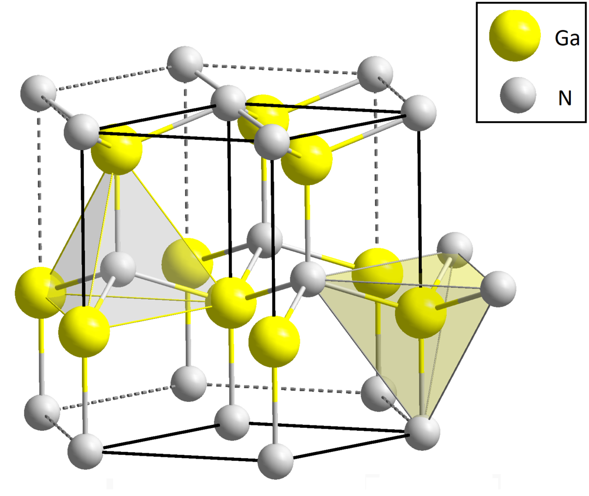
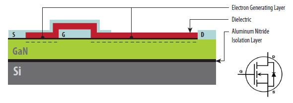
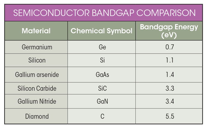
Galliumnitride (GaN) power transistors switch faster and have lower onresistance than conventional silicon MOSFETs Compared to silicon, and even siliconcarbide (SiC) transistors, GaN devices. Gallium nitride (Ga N) is a binary III/V direct bandgap semiconductor commonly used in blue lightemitting diodes since the 1990s The compound is a very hard material that has a Wurtzite crystal structureIts wide band gap of 34 eV affords it special properties for applications in optoelectronic, highpower and highfrequency devices For example, GaN is the substrate which makes violet (405. The smaller die size of a GaN FET, compared to a silicon MOSFET, enables performance improvements in switching power applications Parasitics such as output capacitance and layout inductance are reduced, leading to reduced switching losses and/or higher frequency operation with the same loss Si S D GaN Dielectric Aluminum Nitride Isolation Layer.
News Alpha and Omega Semiconductor Introduces 4Channel UltraLow Capacitance UltraLow Clamping Voltage TVS Arraymore ». VisIC’s industryleading GaN power transistors are the building blocks of unparalleled efficiency gains in the powertrain of electric cars The D 3 GaN technology semiconductors allow for smaller, lower cost, more efficient systems, extending the range of electric cars. Gallium Nitride Wide BandGap HEMT Empower RF has broad experience delivering high power GaN amplifiers into mission critical applications and was a very early adopter of GaN on SiC Although Empower has many product lines encompassing stateoftheart Bipolar, MOSFET, LDMOS and GaAs FET devices, GaN has become the marquee technology for TWT.
GaN transistors can switch much faster than silicon MOSFETs which offers the potential to achieve lower switching losses Our GaN transistors are being adopted for a wide range of applications from telecommunications, servers, motor drives, laptop adapters and onboard chargers for electric vehicles. A wellconsidered selection of the MOSFET defines the overall performance Due to its simplicity and robustness, Infineon’s gamechanging technology is the best choice as it enables improved form factors and contributes to an overall system cost reduction. The GANWSA is a 650 V, 50 mΩ Gallium Nitride (GaN) FET It is a normallyoff device that combines Nexperia’s stateoftheart highvoltage GaN HEMT and lowvoltage silicon MOSFET technologies — offering superior reliability and performance.
GaN switching devices are available in two types enhancement mode (eGaN) and cascoded depletion mode (dGaN) An eGaN transistor works as a normal MOSFET, even with a reduced gatetosource voltage It offers a simpler package and low resistance, with a bidirectional channel and without a body diode. The GaN transistor structure is a purely lateral device, without the parasitic bipolar junction common to silcon MOSFETs Therefore, the enhancement GaN reverse bias or “diode” operation has a different mechanism, but a similar function With zero bias gatetosource there is an absence of electrons under the gate region. The TPH3212PS 650V 72mΩ Gallium Nitride (GaN) FET is a normallyoff device It combines stateoftheart high voltage GaN HEMT and low voltage silicon MOSFET technologies—offering superior reliability and performance.
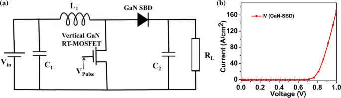
GaN The temperature coefficient of a GaN FET’s onresistance is positive like the silicon MOSFET, but the magnitude is significantly less Compared to a silicon semiconductor, GaN’s higher electron mobility enables a smallersize device for a given onresistance and breakdown voltage. We demonstrate for the first time the monolithic integration of vertical GaN MOSFETs with freewheeling Schottky barrier diodes (SBD), based on a 67μmthick npn heterostructure grown on 6inch silicon substrates by metal organic chemical vapor deposition The anode of the SBD is integrated in the source pad of the MOSFET and the cathode is directly connected to the MOSFET drain through the. The leading candidate for taking electronic performance to the next level and a reactivation of positive momentum of Moore’s Law is gallium nitride GaN’s ability to conduct electrons more than 1000 times more efficiently than silicon, while being able to be manufactured at a lower cost than silicon has now been well established Silicon is out of gas, and a new, higher performing semiconductor material is emerging – GaN is on the rise.
Gallium nitride (GaN) continues to ramp into $B silicon chip market DUBLIN, Ireland (PRWeb) Navitas Semiconductor today announced they have been awarded ASPENCORE’s Electronic Products’ “Power Product of the Year” Navitas’ GaN Power IC NV612x series was. The TPH3212PS 650V 72mΩ Gallium Nitride (GaN) FET is a normallyoff device It combines stateoftheart high voltage GaN HEMT and low voltage silicon MOSFET technologies—offering superior reliability and performance. Failure rates across our existing portfolio of Discretes, MOSFETs and Analog & Logic ICs We extend our AECQ101 qualification into our GaN FETs development 2 Nexperia Power GaN FETs Si 2790nC 600 60 0 0 400 40 0 0400 40 GaN FETs enable smaller, faster, cooler, lighter systems, with lower overall system cost Where.
As discussed in detail in Chapter 14 of the book, “GaN Transistors for Efficient Power Conversion”, there are no insurmountable barriers to achieving an even lower cost for an equivalent performance eGaN FET compared with a power MOSFET or IGBT Basic GaN FET Structure The basic GaN transistor structure is shown in Figure 5. Download or order your hardcopy of the MOSFET and GaN FET Application Handbook A Power Design Engineer’s Guide The second edition to the hugely popular MOSFET application handbook, the updated version is a unique collection of technical materials and application notes providing essential and uptodate information for anybody tasked with integrating MOSFETs and GaN FETs into realworld. The GSB is an enhancement mode GaNonsilicon power transistor The properties of GaN allow for high current, high voltage breakdown and high switching frequency GaN Systems innovates with industry leading advancements such as patented Island Technology® and GaNPX® packaging.
VisIC’s industryleading GaN power transistors are the building blocks of unparalleled efficiency gains in the powertrain of electric cars The D 3 GaN technology semiconductors allow for smaller, lower cost, more efficient systems, extending the range of electric cars. GaN is a very hard (Knoop hardness 1421 GPa), mechanically stable wide bandgap semiconductor material with high heat capacity and thermal conductivity In its pure form it resists cracking and can be deposited in thin film on sapphire or silicon carbide, despite the mismatch in their lattice constants. News Alpha and Omega Semiconductor Announces New High SOA MOSFETs for 48V Hot Swap Telecom Applicationsmore »;.
GaN FET Drivers 3 Products Parametric Search Parametric Search Description Configuration Max Vin (V) Frequency (MHz) Rise Time (ns) Fall Time (ns) Propagation Delay (ns) Min Output Pulse Width (ns) Deadtime Control Features Package Package (mm) PE PE Highspeed FET Driver High and lowside FET drivers. The portfolio of Gate Drivers from ON Semiconductor includes GaN, IGBT, FET, MOSFET, HBridge MOSFET, and SiC MOSFET inverting and noninverting drivers ideal for switching applications ON Semiconductor Gate Drivers provide features and benefits that include High system efficiency high reliability, High Current Output at IGBT Miller Plateau. GaN MOSFET are available at Mouser Electronics Mouser offers inventory, pricing, & datasheets for GaN MOSFET.
Si MOSFET can’t be used for any half bridge hardswitch circuit due to Q RR Excellent reverse recovery of GaN enables new topologies such as bridgeless totem pole PFC V DS V GS Ι D Math V DS * Ι D Half bridge turnon 400V/A – SJ MOSFET Half bridge turnon 400V/A – GaN EHEMT Si MOSFET Q RR Loss = 6670uJ!. Gallium nitride (GaN) offers fundamental advantages over silicon In particular, the higher critical electrical field makes it very attractive for power semiconductor devices with outstanding specific dynamic onstate resistance and smaller capacitances compared to silicon MOSFETs, which makes GaN HEMTs great for high speed switching.
Gallium Nitride Wikipedia
Materials Free Full Text Fabrication And Evaluation Of N Channel Gan Metal Oxide Semiconductor Field Effect Transistors Based On Regrown And Implantation Methods Html

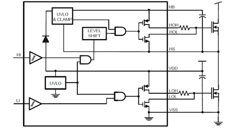
Lmg1210 Half Bridge Mosfet Gan Fet Driver Ti Digikey
Top Down Gan Nanowire Transistors With Nearly Zero Gate Hysteresis For Parallel Vertical Electronics Scientific Reports
This Is The Structural Design Of The Gan Mosfet Where The Variables Download Scientific Diagram

Cross Sectional Schematic Of Normally Off Gan Mosfet With P Gan Download Scientific Diagram
Power Gan Products Resources Digi Key Electronics Digikey

How To Gan Intro To Gallium Nitride Gan Transistor Technology
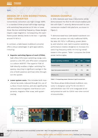
Page 42 Special Project Gan Sic

Improving Reliability For Gan And Sic

Design And Evaluation Of Cascode Gan Fet For Switching Power Conversion Systems Jung 17 Etri Journal Wiley Online Library
100 V Egan Fet Family
600 V Gan Hemt Targets Pfc Off Line Power Supply Electronic Products

Yole Yole Developpement Yole Development System Plus Consulting System Plus Power Power Electronic Power Electronics Inverter Device Component Wafer Level Wafer Substrate Gan Sic Gallium Nitride Silicon Carbide Mosfet Igbt Discrete

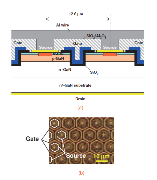
Toshiba Corporate Research Development Center Toshiba Develops A Gate Dielectric Process Technology For Improving The Reliability Of Gan Mosfet
Gan Basics Faqs Power Electronics

Sciencecentral

Structure Of The Investigated Gan Mosfet With Selected Breakdown Regions Download Scientific Diagram
What You Need To Know About Gan For Power Conversion Applications Electrical Engineering News And Products

Mouser Lmg1210 Mosfet And Gan Fet Driver For High Frequency Applications Iaa Industrial Automation

Gan Power Devices Part 1 Principles
Q Tbn And9gctmpchqoi1popszqu9tlxy Cjfkjspdixmztdn Ohyxkoxxpsq Usqp Cau

Mosfet And Gan Fet Application Handbook Efficiency Wins

Gan Power Devices Potential Benefits And Keys To Successful Use Mouser
What Is Gan

Using Mosfet Controllers To Drive Gan Ehemts Technical Articles
Gan Based Transistor Blocking Voltage Exceeds 1kv

1 Hfo2 Gan Dg Mosfet Structure Figure 4 1 Gan Dg Mosfet Showing Download Scientific Diagram
Q Tbn And9gcsg4hnaeisbnfc7r5wx3rxid73p8snj6r6d9koezuq9ptn3pn5q Usqp Cau
Increasing Gallium Nitride Mosfet Threshold Voltage
Gansystems Com Wp Content Uploads 01 Using Mosfet Controllers To Drive Gan Ehemts Pdf
Compoundsemiconductor Net Article 1028 Gan Power Devices Perfecting The Vertical Architecture Feature

Figure 2 From 600 V Gan Vertical V Trench Mosfet With Mbe Regrown Channel Semantic Scholar
Considerations When Comparing Sic And Gan In Power Applications

Power Gan Products Resources Digi Key Electronics Digikey
Www Infineon Com Dgdl Infineon How 600v Gan Transistors Improve Power Supply Efficiency And Density Art V01 00 En Pdf Fileid 5546dad12b5a

Improvement Of Device Isolation Using Field Implantation For Gan Mosfets Iopscience
Gan Is Like A Ferrari How Gan Is On The Fast Track For 21 News

Gallium Nitride Gan Technology Overview Edn

Gan Fet Vs Mosfet 48 V 1 8 V Dc Dc Conversion

Isolated Gate Drivers For Gan Mosfets Ee Times Europe
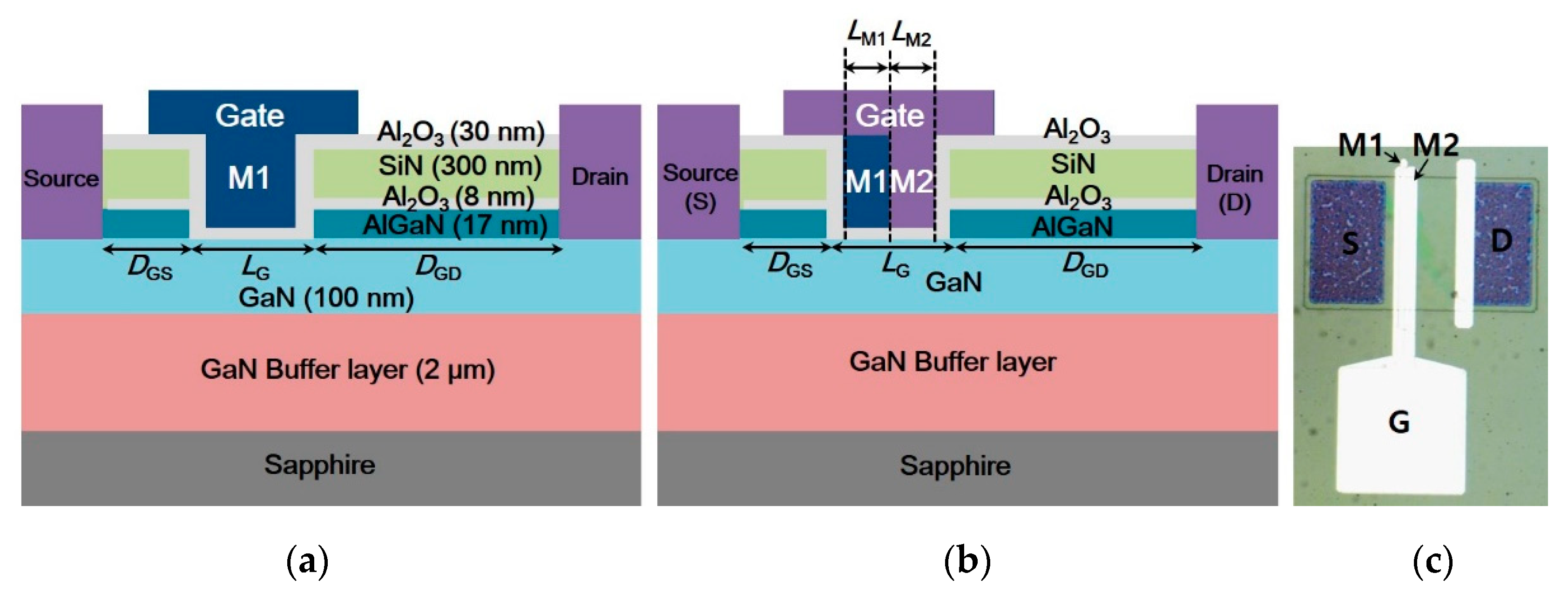
Electronics Free Full Text Gallium Nitride Normally Off Mosfet Using Dual Metal Gate Structure For The Improvement In Current Drivability

Gan Vs Mosfet Youtube

Color Online Cross Section Of The Fabricated Gan Mosfet And Mos Hemt Download Scientific Diagram

Gan Type Determines Design Benefits
Gallium Nitride Brings Sound Quality And Efficiency To Class D Audio

A Study On The Impact Of Channel Mobility On Switching Performance Of Vertical Gan Mosfets Semantic Scholar
Materials Free Full Text Fabrication And Evaluation Of N Channel Gan Metal Oxide Semiconductor Field Effect Transistors Based On Regrown And Implantation Methods Html
Power Tips How Gan Devices Boost Resonant Converter Efficiency Power Management Technical Articles Ti E2e Support Forums
Q Tbn And9gcs4rtymid3ady96asmopt0wlwcdkklhpe S8chalnbc9r7h4zeo Usqp Cau

Gan Fet Driver Ics
Market Analysis Who Really Requires Gan Sic Power Devices
Gan Nexperia
Gan On Si Hemt Vs Sj Mosfet Technology And Cost Comparison Teardo

Driver Ic Optimises Class D Audio Amps With Gan Output Fets

Design Of High Power Devices With Gan Power Electronics News
Radiation Performance Of Enhancement Mode Gan Power Devices Technical Articles
Epc Doubles The Performance Of Its 0 V Egan Fet Family Business Wire

Gan Devices Bring Benefits To Pol Dc Dc Converter Designs Electronic Design

Gan Technology Is Coming Of Age As Power Consumption Grows Applied Materials

Fig1 1 Cross Section View Of Basic Algan Gan Hemt Gan Mosfet And How Download Scientific Diagram
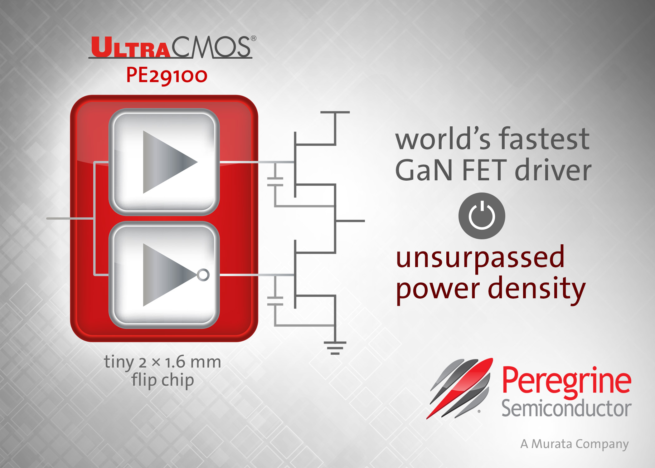
Peregrine Semiconductor Unveils The World S Fastest Gan Fet Driver Psemi

Sciencecentral

Gan Hemts Outperform Mosfets In Key Growth Applications Ee Times Europe

Performance
Medium Voltage Gan Hemt Vs Superjunction Mosfet Comparison 19 System Plus Consulting

Vertical Gan Devices For A New Power Electronics Power Electronics News
Gan Is Like A Ferrari How Gan Is On The Fast Track For 21 News
An003 Using Enhancement Mode Gan On Silicon Power Fets

Gan Fets Step Up Performance Cut Package Footprint

Mega Electronics Announces Launch Of Gan Fet Power Supplies Astute Electronics

Gallium Nitride Based Device Technology Namlab

Panasonic To Start Mass Production Of Gan Power Transistor Drivers

Das Unterscheidet Die Bauelementekonzepte Gan Sic Superjunction All Electronics

Yole Yole Developpement Yole Development System Plus Consulting System Plus Power Power Electronic Power Electronics Inverter Device Component Wafer Level Wafer Substrate Gan Sic Gallium Nitride Silicon Carbide Mosfet Igbt Discrete

Mosfet Or Igbt Igbt Vs Mosfet Explanations

Thoughtful Board Design Unlocks The Promise Of Gan Electronic Design

Yole Yole Developpement Yole Development System Plus Consulting System Plus Power Power Electronic Power Electronics Inverter Device Component Wafer Level Wafer Substrate Gan Sic Gallium Nitride Silicon Carbide Mosfet Igbt Discrete
Gan Mosfet的工作原理及结构设计 Ganhemt氮化镓科技汇
Medium Voltage Gan Hemt Vs Superjunction Mosfet Comparison 19 System Plus Consulting
Vertical Gan Reverse Trench Gate Power Mosfet And Dc Dc Converter Springerlink
Vertical Gan Transistor With 1 6kv Blocking Voltage
First Quasi Vertical Gallium Nitride Trench Mosfet On Six Inch Silicon

Sic Mosfet And Gan Fet Switching Power Converter Analysis Kit Tektronix
1

Gan Thyristors And Mosfets Stephen J Pearton University Of

Texas Instruments Optimizing Gan Performance With Integrared Driver

Sic Mosfet And Gan Fet Switching Power Converter Analysis Kit Tektronix
Transphorming The Power Transistor Industry Using Gan I Micronews

900v 170mw Gallium Nitride Gan Fet Transphorm Mouser
Vertical Gan Reverse Trench Gate Power Mosfet And Dc Dc Converter Springerlink

Gan Fet Vs Mosfet 150 V 12 V Dc Dc Conversion Youtube
Gan041 650wsb 650 V 35 Mw Gallium Nitride Gan Fet In A To 247 Package Nexperia
High Quality Mos Transisotor Gan Fet 30v 90a To 252 Buy Gan Mosfet Mos Transisotor 90a Mosfet Product On Alibaba Com

Lmg1210 0v Half Bridge Mosfet Gan Fet Drivers Ti Mouser
The Great Semi Debate Sic Or Gan Power Electronics

Charged Evs Sic Vs Gan Semiconductors For Ev Power Converters Tech Opinion Charged Evs
Class D Amplifiers 101 Page 2 Audio Science Review Asr Forum


